You must choose between Dual Inline Package (DIP) and Surface Mount Technology (SMT). The choice depends on factors related to your application, manufacturing, and design. Here’s a comparison to help you decide:
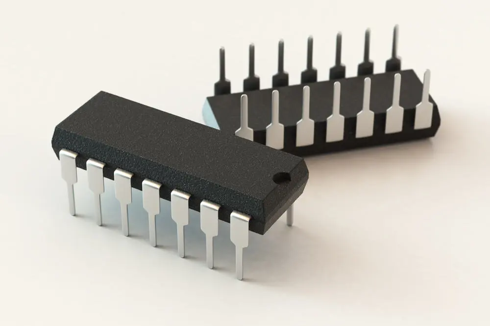
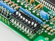
Dual Inline Package (DIP)
Overview
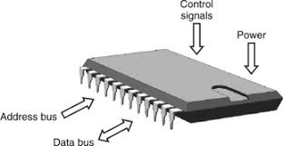
DIP is a through-hole mounting technology. The leads of the electronic component are put into holes in the PCB. They are then soldered on the opposite side.
Components are usually larger. They have leads (pins) extending from the body. This makes them good for manual insertion and soldering.
Advantages
DIP technology offers several advantages. This is true, especially in some applications and manufacturing contexts. Here are some key advantages of dual in package components
Mechanical Strength and Durability
DIP components are mechanically strong due to their through-hole mounting method. The leads (pins) are put through holes in the PCB. They are soldered on the other side. This forms a strong mechanical bond.
Ease of Prototyping and Testing
DIP packages are easier to prototype and test by hand. This is compared to surface mount technology (SMT). Parts can be easily put in and removed from the PCB. This helps fast iteration and debugging in development.
Higher Power Handling
DIP components have bigger leads. They can handle more current than similarly sized SMT components.
Accessibility and Repairability
DIP components are easier to solder and fix by hand. This is in contrast to SMT components. SMT components often need special equipment and techniques.
Wide Availability and Compatibility
DIP components have been widely used and standardized for decades. This makes them readily available in many types, sizes, and specs. They work with standard PCB manufacturing and assembly. They are compatible with existing infrastructure.
Noise Reduction
In some cases, DIP packages can offer better noise reduction than SMT components. This is due to how they are made and mounted. This can be beneficial in analog and sensitive electronic circuits.
Disadvantages
Size and Space
DIP components take up more space on the PCB than SMT components. This limits PCB space for dense designs.
Limitations in High-Frequency Designs
DIP packages are bad for high-frequency. This is due to their long leads. The leads can add parasitic capacitance and inductance.
Manual Assembly
People usually put together DIP components by hand. This can be slower and less cost-effective for large-scale production.
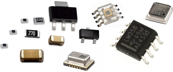
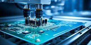
Surface Mount Technology (SMT)
Overview
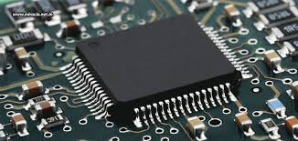
SMT involves mounting parts directly on the surface of the PCB. This is done without leads passing through holes.
Components are smaller. They have metalized contacts, called pads. The pads stick to solder paste on the PCB during reflow soldering.
Advantages
Size and Weight Reduction
SMT components are significantly smaller and lighter compared to their through-hole counterparts. This miniaturization allows for higher component density on circuit boards, leading to smaller and more compact electronic devices.
Improved Electrical Performance
SMT components are mounted closer to the surface of the PCB, resulting in shorter interconnection paths. This reduces parasitic capacitance, inductance, and resistance, thereby improving signal integrity and reducing signal loss.
Enhanced Manufacturing Efficiency
SMT components are mounted using automated pick-and-place machines, which significantly speeds up the assembly process compared to manual insertion of through-hole components.
Cost-Effectiveness
SMT technology requires fewer materials (e.g., PCB substrate, solder) compared to THT, resulting in cost savings, especially for high-volume production runs.
Reduced Labor Costs
Automated SMT assembly reduces labor costs associated with manual component insertion and soldering, optimizing production efficiency and reducing operational expenses.
Reliability and Durability
SMT components are mechanically secured to the PCB using solder joints and adhesive bonding, offering better shock and vibration resistance compared to through-hole components.
Design Flexibility and Innovation
SMT technology allows for greater design flexibility and innovation in PCB layout, enabling designers to create complex, multi-layered circuits with reduced space constraints.
Environmental Benefits
SMT technology supports lead-free soldering processes, complying with environmental regulations and promoting safer manufacturing practices.
Disadvantages
Mechanical Durability
SMT components may be less mechanically robust compared to DIP components, especially under high mechanical stress or vibration.
Prototyping Challenges
Initial prototyping and testing of SMT designs may require specialized equipment and processes compared to DIP.
Heat Dissipation
SMT components may have challenges in heat dissipation due to their smaller size and closer proximity to the PCB surface.
Choosing Between DIP and SMT
Application Requirements
Consider the electrical and mechanical requirements of your application. If robustness and mechanical strength are critical, DIP may be preferable. For high-frequency or compact designs, SMT is generally more suitable.
Production Scale
If you anticipate large-scale production with automated assembly, SMT offers efficiency advantages. For smaller-scale production or prototyping, DIP might be more accessible.
Design Constraints
Evaluate PCB space constraints and the need for component miniaturization. SMT allows for denser PCB layouts and smaller overall product size.
Check out best PCB Assembly service here: https://kingsunpcba.com/
Conclusion
In conclusion, the choice between DIP and SMT depends on your specific application needs, production scale, and design constraints. Both technologies have their strengths and considerations, so it’s essential to weigh these factors carefully to determine the best fit for your project.
Stay in touch to get more updates & news on Discover Tribune!